Nanoscale Manufacturing Techniques
Nanoscale manufacturing techniques are a set of processes and tools used to create structures and devices with dimensions on the nanometer scale, typically between 1 and 100 nanometers. These techniques are crucial for the development of na…
Nanoscale manufacturing techniques are a set of processes and tools used to create structures and devices with dimensions on the nanometer scale, typically between 1 and 100 nanometers. These techniques are crucial for the development of nanotechnology, which has the potential to revolutionize many industries, including textile engineering. In this explanation, we will discuss some of the key terms and vocabulary related to nanoscale manufacturing techniques in the context of the Masterclass Certificate in Nanotechnology for Textile Engineering.
1. Nanoscale: The nanoscale refers to the size range of 1 to 100 nanometers. A nanometer is one billionth of a meter, which is about 10,000 times smaller than the width of a human hair. At the nanoscale, materials exhibit unique properties that differ from their bulk counterparts, such as increased strength, altered electrical conductivity, and novel optical properties. 2. Nanofabrication: Nanofabrication is the process of creating nanoscale structures and devices using various techniques. Nanofabrication is a multidisciplinary field that combines elements of physics, chemistry, materials science, and engineering. Nanofabrication techniques can be divided into two categories: top-down and bottom-up. 3. Top-down nanofabrication: Top-down nanofabrication involves using lithographic techniques to etch or remove material to create nanoscale structures. Lithography is a process that uses light, electrons, or ions to pattern a material. The most commonly used lithographic technique is photolithography, which uses ultraviolet light to transfer a pattern from a mask to a photosensitive material. 4. Bottom-up nanofabrication: Bottom-up nanofabrication involves assembling nanoscale components into larger structures. This can be achieved through various techniques, such as self-assembly, electrostatic assembly, and molecular beam epitaxy. 5. Self-assembly: Self-assembly is a process in which nanoscale components spontaneously organize themselves into larger structures. This can be achieved through various mechanisms, such as electrostatic interactions, van der Waals forces, and hydrogen bonding. 6. Electrospinning: Electrospinning is a nanofabrication technique used to create ultrafine fibers with diameters ranging from a few nanometers to several micrometers. Electrospinning involves applying a high voltage to a polymer solution or melt, which creates an electrically charged jet that is collected on a grounded target. 7. Nanolithography: Nanolithography is a subset of lithography that deals with creating patterns with features on the nanoscale. Nanolithography techniques include photolithography, electron beam lithography, and nanoimprint lithography. 8. Photolithography: Photolithography is a nanolithography technique that uses ultraviolet light to transfer a pattern from a mask to a photosensitive material. Photolithography is the most commonly used technique for manufacturing microelectronics, but it is limited by the diffraction limit of light, which sets a minimum feature size of about 100 nanometers. 9. Electron beam lithography: Electron beam lithography is a nanolithography technique that uses a focused beam of electrons to write patterns directly onto a resist-coated substrate. Electron beam lithography can create features with dimensions as small as a few nanometers, making it a powerful tool for nanofabrication. 10. Nanoimprint lithography: Nanoimprint lithography is a nanolithography technique that uses a mold to mechanically stamp a pattern onto a resist-coated substrate. Nanoimprint lithography can create features with dimensions as small as a few nanometers, making it a cost-effective alternative to electron beam lithography. 11. Nanostructures: Nanostructures are materials that have been engineered to have dimensions on the nanoscale. Nanostructures can be created using top-down or bottom-up nanofabrication techniques. Nanostructures can exhibit unique properties that differ from their bulk counterparts, such as increased strength, altered electrical conductivity, and novel optical properties. 12. Carbon nanotubes: Carbon nanotubes are a type of nanostructure made
of carbon atoms arranged in a cylindrical shape. Carbon nanotubes can have diameters as small as one nanometer and lengths up to several micrometers. Carbon nanotubes exhibit unique electrical, mechanical, and thermal properties, making them useful for a variety of applications, including textile engineering.
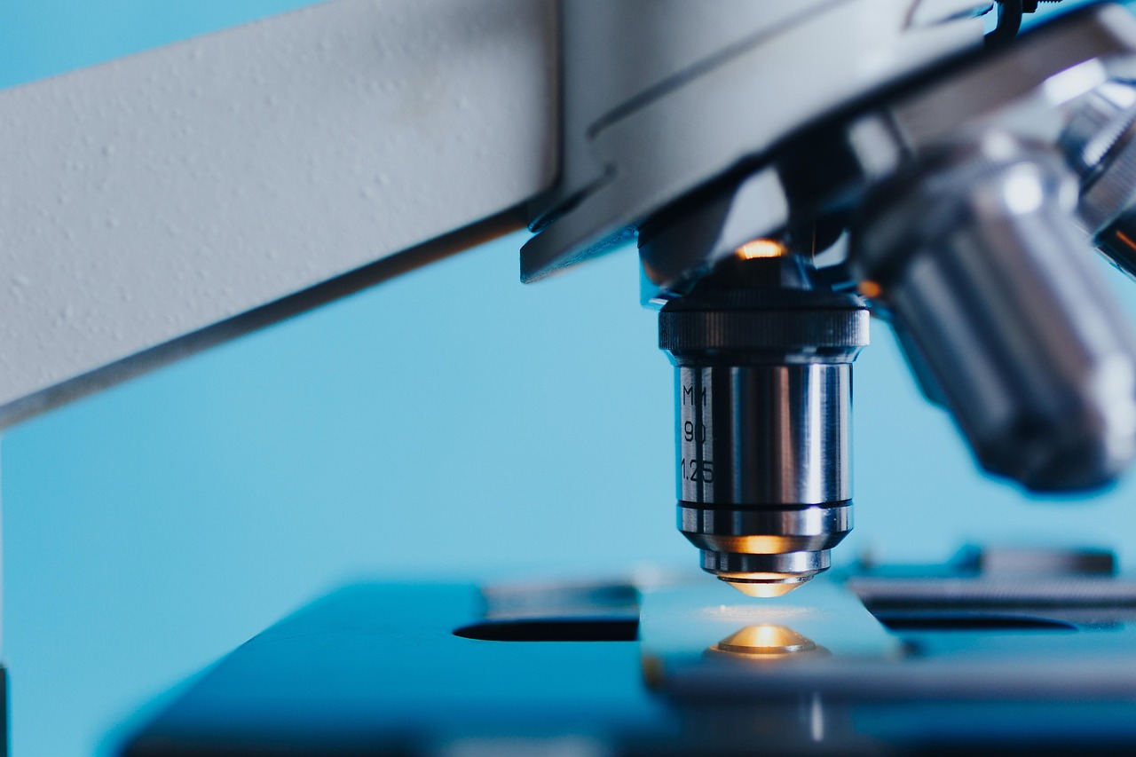
1. Graphene: Graphene is a single layer of carbon atoms arranged in a two-dimensional lattice. Graphene is the thinnest and strongest material known, with a tensile strength 200 times greater than steel. Graphene also exhibits unique electrical and thermal properties, making it a promising material for a variety of applications, including textile engineering. 2. Quantum dots: Quantum dots are nanoscale semiconductor particles that exhibit unique optical properties. Quantum dots can emit light in a range of colors, depending on their size and composition. Quantum dots are used in various applications, such as displays, medical imaging, and solar cells. 3. Nanocomposites: Nanocomposites are materials that consist of a matrix material and nanoscale reinforcements. Nanocomposites exhibit unique properties that differ from their bulk counterparts, such as increased strength, altered electrical conductivity, and novel optical properties. Nanocomposites are used in various applications, including textile engineering. 4. Nanoencapsulation: Nanoencapsulation is a process in which nanoparticles are encapsulated in a protective coating. Nanoencapsulation is used to protect nanoparticles from degradation and to control their release. Nanoencapsulation is used in various applications, such as drug delivery, food packaging, and cosmetics. 5. Nanoinstrumentation: Nanoinstrumentation is the set of tools and techniques used to measure and manipulate nanoscale structures and devices. Nanoinstrumentation includes techniques such as atomic force microscopy, scanning tunneling microscopy, and transmission electron microscopy. 6. Atomic force microscopy (AFM): Atomic force microscopy is a nanoinstrumentation technique used to image and manipulate nanoscale structures. AFM uses a sharp probe to scan the surface of a sample, and the probe's deflection is used to create a topographic image of the surface. 7. Scanning tunneling microscopy (STM): Scanning tunneling microscopy is a nanoinstrumentation technique used to image and manipulate nanoscale structures. STM uses a sharp probe to scan the surface of a sample, and the probe's tunneling current is used to create a topographic image of the surface. 8. Transmission electron microscopy (TEM): Transmission electron microscopy is a nanoinstrumentation technique used to image and analyze nanoscale structures. TEM uses a beam of electrons to transmit through a thin sample, and the resulting image is magnified to reveal details on the nanoscale.
In conclusion, nanoscale manufacturing techniques are a set of processes and tools used to create structures and devices with dimensions on the nanometer scale. These techniques are crucial for the development of nanotechnology, which has the potential to revolutionize many industries, including textile engineering. Key terms and vocabulary related to nanoscale manufacturing techniques include nanoscale, nanofabrication, top-down nanofabrication, bottom-up nanofabrication, self-assembly, electrospinning, nanolithography, photolithography, electron beam lithography, nanoimprint lithography, nanostructures, carbon nanotubes, graphene, quantum dots, nanocomposites, nanoencapsulation, nanoinstrumentation, atomic force microscopy, scanning tunneling microscopy, and transmission electron microscopy. Understanding these key terms and concepts is essential for anyone pursuing a Masterclass Certificate in Nanotechnology for Textile Engineering.
Challenges:
1. What are the advantages and limitations of top-down and bottom-up nanofabrication techniques? 2. How are carbon nanotubes and graphene used in textile engineering? 3. What are the differences between photolithography, electron beam lithography, and nanoimprint lithography? 4. How are nanostructures used in the development of nanotechnology? 5. What are quantum dots and how are they used in various applications? 6. What are nanocomposites and how do they exhibit unique properties compared to their bulk counterparts? 7. What is nanoencapsulation
Key takeaways
- In this explanation, we will discuss some of the key terms and vocabulary related to nanoscale manufacturing techniques in the context of the Masterclass Certificate in Nanotechnology for Textile Engineering.
- Photolithography is the most commonly used technique for manufacturing microelectronics, but it is limited by the diffraction limit of light, which sets a minimum feature size of about 100 nanometers.
- Carbon nanotubes exhibit unique electrical, mechanical, and thermal properties, making them useful for a variety of applications, including textile engineering.
- Nanocomposites exhibit unique properties that differ from their bulk counterparts, such as increased strength, altered electrical conductivity, and novel optical properties.
- In conclusion, nanoscale manufacturing techniques are a set of processes and tools used to create structures and devices with dimensions on the nanometer scale.
- What are the differences between photolithography, electron beam lithography, and nanoimprint lithography?